University of Michigan
Lurie Nanofabrication Facility
University of Michigan, Ann Arbor, Michigan
Expertise: MEMS, Electronics, System Integration, Biological Sensors, Nanoscale Computation, Geosciences
The Lurie Nanofabrication Facility (LNF) at the University of Michigan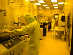 is one of the leading centers worldwide on micro electromechanical systems (MEMS) and microsystems. It provides facilities and processes for the integration of Si integrated circuits and MEMS with nanotechnology, with applications in biology, medical systems, chemistry, and environmental monitoring. The LNF builds on its experience in integration of Si-based electronics with MEMS transducers and micropackaging to push these interfaces into the nanometer regime with emphasis on the fabrication, packaging, and testing of integrated devices for chemical and biological sensing, electrical stimulation of biological systems, and integrated fluidic systems.
The facility is run by a laboratory manager together with a staff of twenty engineers and technicians, who are responsible for ensuring that the equipment is well maintained and characterized. It consists of a Class 1000/100/10 research laboratory available 24/7 with approximately 12,500 square feet of work area.
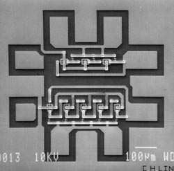
Research is focused on the theory, design, and fabrication of electronic, optoelectronic, and micromachined devices, circuits, and microsystems, as well as on novel characterization and metrology techniques. The Lurie Nanofabrication Facility offers a complete laboratory for the fabrication of solid-state MEMS and integrated circuits. In the Si circuits area, an E/D Si-gate NMOS process and a 3 µm double-poly single-metal p-well CMOS, and a companion BiCMOS process are available for use as needed. All major MEMS fabrication technologies are available - bulk, surface, polymer/plastic, and molded electroplated micromachining. III-V compound capabilities are available for research on high-speed micro-, nano-, and opto-electronics, including microwave/millimeter wave devices and circuits, and integrated optical devices. The LNF has in-house characterization ability (SEM, spectroscopic ellipsometry, AFM and profilometry).
 For Information and Access Contact:
Sandrine Martin
User Manager
734-763-6719
sandrine\AT/umich.edu