University of California at Santa Barbara
Nanotech
University of California at Santa Barbara, Santa Barbara, California
Expertise: Optics and Electronics Materials
UCSB has extensive facilities and research in nanotechnology. 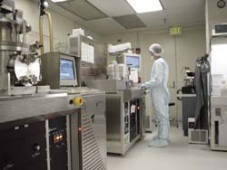 Specific UCSB strengths include leading expertise in compound semiconductors, photonics, quantum structures, and expertise with non-standard materials and fabrication processes. Research within the UCSB research community is highly collaborative, involving Materials Science, Chemistry, Physics, Biology, and Chemical Electrical and Mechanical Engineering. Areas of excellence include: compound semiconductor electronic and optoelectronic devices in GaAs, InP and the semiconductor nitrides; polymer and organic electronic and photonic devices; quantized electron structures and THz physics; spintronics, single electronics, and quantum computation; quantum optics; MEMS/NEMS, bio-instruments, and microfluidics.
The nanofabrication facility has comprehensive and advanced semiconductor and thin film processing equipment and provides access and professional consultation to industrial and internal and external academic users. The facility currently consists of 12,700 ft2 of class 100 and 10,000 clean space.
A wide range of materials including silicon, compound semiconductors (III-V in particular), and novel and unusual materials (including polymers and ceramics) are processed in the facility. All lithographic systems have tooling for most substrate shapes, including small and irregular shapes and sizes.
A new JEOL 6300, 100kV system capable of writing sub-10 nm features is fully operational. These tools are a foundation for nm-scale scientific exploration and technology development for a wide range of materials and devices. Dry etch capabilities are a particular strength, with eight reactive-ion-etch systems (including four advanced inductively-coupled plasma systems) available for etching many types of semiconductors, metals, and dielectrics. Thin films of metals and dielectrics are deposited onto a variety of host substrate materials by an extensive tool set including sputtering, reactive sputtering, electron-beam and thermal evaporation, and plasma-based CVD systems.
The facility also houses many benches and systems for chemical processing, substrate preparation and cleaning, rapid thermal processing, oven curing, wafer cutting, and thin-film and device characterization. Both on-site and remote support of users (including equipment training, process consultation, and remote job processing) is provided by our staff, consisting of six engineers supporting facilities and three Ph.D.-trained engineers supporting process.
For Information and Access Contact:
Brian Thibeault
(805)893-2268
thibeault@ece.ucsb.edu