Photocurable Nanoimprint (P-NIL) Process for Patterning Nitride and Oxide (Cornell)
Vincent Genova, Process Engineer, Cornell
Posted Dec. 2012
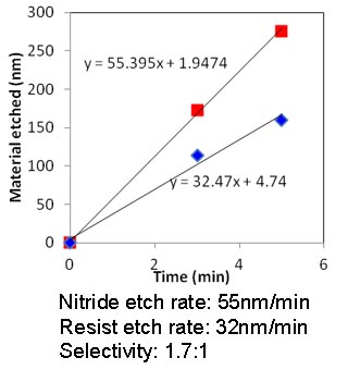
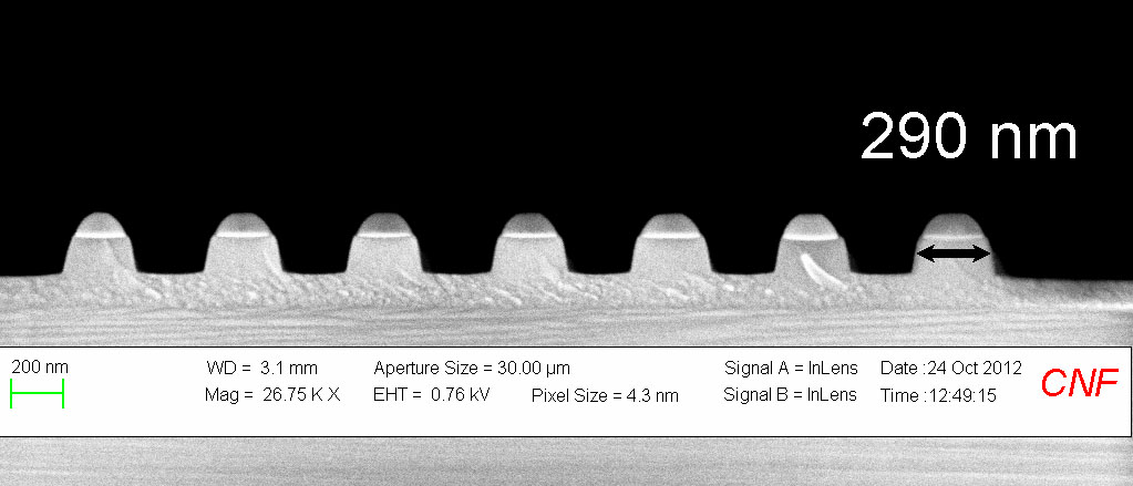
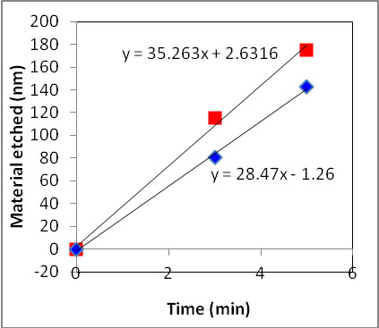
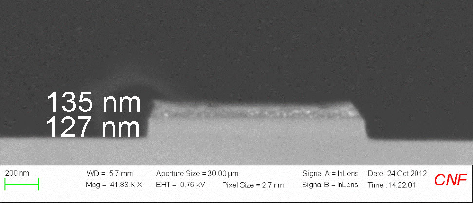
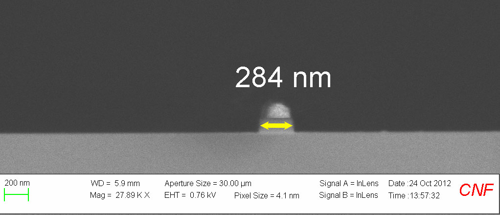
The recently established photocurable nanoimprint (P-NIL) process has been demonstrated with pattern transfer into silicon oxide and silicon nitride using an internally fabricated ASML DUV (248nm) patterned quartz template. The P-NIL process utilizes a bilayer resist system in which the first resist layer (200nm) is purely organic, while the upper UV resist layer (90nm) contains silicon. After imprint, the pattern transfer starts with a residual layer etch whose thickness is dependent on geometrical feature layout and applied pressure. A selective fluorocarbon etch chemistry is used for the residual layer, while oxygen is used to etch the underlying purely organic transfer layer. These etches must preserve the critical dimensions (CD) defined by the imprint process. The imprint pattern is then successfully transferred into the underlying thermal silicon dioxide film using CHF3/O2 chemistry using the Oxford 80 conventional RIE system and the advanced ICP based Oxford 100 system with etch rates of 35nm/min and 127nm/min and selectivities to resist of 1.3:1 and 5:1 respectively. This etch was successfully demonstrated with feature sizes as small as 200nm. Similarly, CHF3/O2 chemistry is used to pattern transfer into underlying LPCVD silicon nitride using both the Oxford 80 and the Oxford 100 ICP systems, with etch rates of 55nm/min and 142nm/min respectively and selectivities between 1.5-2.0:1. Again features down to 200nm were successfully patterned.
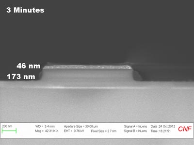
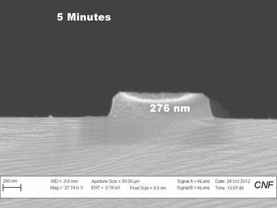
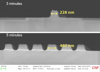
Nitride Oxford 80 (standard RIE) Etches (50/5sccm CHF3/O2, 150W, 55mT) |
||
 |
 |
|
 |
 |
|
Nitride Oxford 100 Etches (ICP) (CHF3/O2 52/2sccm 2500W/50W 6mtorr) |
||
 |
 |
|
|
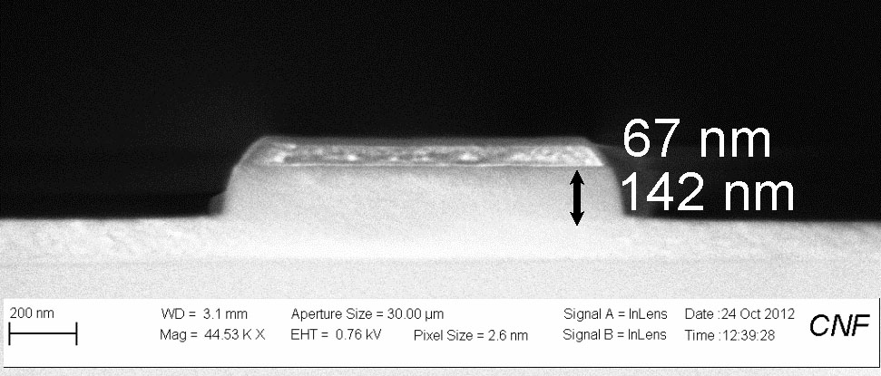
Nitride etch rate: 142nm/min |
||
Oxide Oxford 80 Etches (50/2sccm CHF3/O2, 240W, 40mT) |
||
 |
 |
|
 |
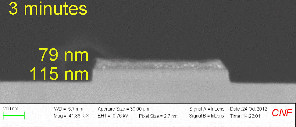
SiO2 etch rate: 35nm/min |
|
Oxide Oxford 100 (ICP) Etches (CHF3/O2 52/2sccm, 2500W/15W, 5mtorr) |
||
 |
 |
|
|
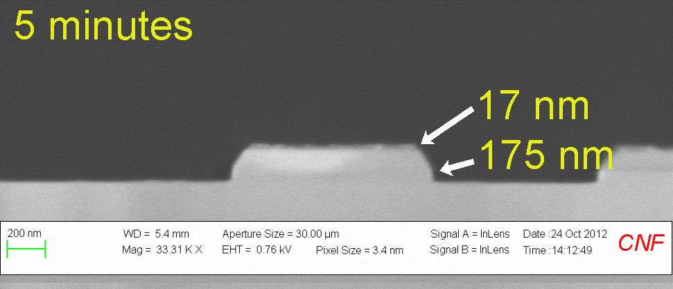
SiO2 etch rate: 127nm/min |
||
- Log in to post comments